
Specification used NVMe V-1.1
- SSD Controller
- SSD Flash
- SSD Interfaces
| System Component | Description | Other information |
| Device Driver(s) | Software created by the OEM to run on the target host processor family under a particular OS and File System. The device driver provides host access the particular SSD product. | Generally device specific, or device family specific, and provided by the OEM. |
| Interface Components | The electrical interface between the host processor and the SSD peripheral device. |
Commonly:
SATA (various), FC, SAS, IDE, PCIe, mPCIe, USB, 1394
|
| SSD Controller | The electronic component(s) that provide SSD device level interfacing and firmware execution. Included is an embedded processor, data ROM, data RAM, flash component interfacing, error correction code (ECC), wear leveling/TRIM, and security features. |
Commonly:
Indilinx IDX110M00-FC
Intel PC29AS21AA0
JMicron JMF612
Samsung S3C29RBB01-YK40
Toshiba T6UG1XBG
SandForce SF-1500
|
| Buffer/Cache Components | This is high speed RAM memory components used for speed matching and to increased data throughput. | Integrated into the Controller in consumer SSDs but are separate components in larger server systems. |
| Controller Firmware |
Software written and stored in electrically erasable memory for execution by the controller. Can be upgraded once in service.
Some advanced techniques include NCQ, TRIM, and wear leveling.
| Device specific and provided by the SSD OEM in most cases. |
| Flash Memory Components | Individual Flash die or devices using either NAND or NOR technology. Densities vary from 2GBytes to 64GBytes. |
Common suppliers:
Toshiba
IMFT (Intel Micron JV)
Samsung
Hynix
|
| Packaging | Various physical form factors |
1.8”, 2.5”, 3.5”, various heights.
SD, CF, USB, PATAZIF
|

Host to SSD Devices
Brief about SSD Controller :
NAND/NOR :
========
The interface provided for reading and writing the memory is different (NOR allows random-access for reading, NAND allows only page access).
Important Terms used in flash memory related devices.
- write amplification
- Flash Translation Layer (FTL)
- logical block mapping
- garbage collection:
- hybrid log-block mapping
The smallest unit through which a block can be read or written is a page. Pages cannot be erased individually, only whole blocks can be erased.
Reading :
======
It is not possible to read less than one page at once.
Writing :
======
When writing to an SSD, writes happen by increments of the page size. So even if a write operation affects only one byte, a whole page will be written anyway. Writing more data than necessary is known as write amplification,
-writing data to a page is sometimes referred to as “to program” a page.
-Page can not be over written:so page that need to be modified is became stale.
Pages cannot be overwritten:
====================
A NAND-flash page can be written to only if it is in the “free” state. When data is changed, the content of the page is copied into an internal register, the data is updated, and the new version is stored in a “free” page, an operation called “read-modify-write”. The data is not updated in-place, as the “free” page is a different page than the page that originally contained the data. Once the data is persisted to the drive, the original page is marked as being “stale”, and will remain as such until it is erased.
Garbage Collection:
==============
Garbage collection is a process cwhich copies all the valid pages from the data block 1000 to free block 2000 leving behind the stale pages.
The erase command is triggered automatically by the garbage collection process in the SSD controller when it needs to reclaim stale pages to make free space.
Wear leveling:
==========
Because NAND-flash cells are wearing off, one of the main goals of the FTL is to distribute the work among cells as evenly as possible so that blocks will reach their P/E cycle limit and wear off at the same time.
Using garbage collection process for achiving wear leaving distributes P/E cycles as evenly as possible among the blocks. Ideally, all blocks would reach their P/E cycle limits and wear off at the same time.
Flash Translation Layer (FTL):
======================
The necessity of having an FTL ?
The main factor that made adoption of SSDs so easy is that they use the same host interfaces as HDDs. Although presenting an array of Logical Block Addresses (LBA) makes sense for HDDs as their sectors can be overwritten, it is not fully suited to the way flash memory works. For this reason, an additional component is required to hide the inner characteristics of NAND flash memory and expose only an array of LBAs to the host. This component is called the Flash Translation Layer (FTL), and resides in the SSD controller. The FTL is critical and has two main purposes: logical block mapping and garbage collection.
Logical block mapping:
=================
It translates logical block addresses (LBAs) from the host space into physical block addresses (PBAs) in the physical NAND-flash memory space. This mapping takes the form of a table, which for any LBA gives the corresponding PBA. This mapping table is stored in the RAM of the SSD for speed of access, and is persisted in flash memory in case of power failure. When the SSD powers up, the table is read from the persisted version and reconstructed into the RAM of the SSD.
- page-level mapping :
- block-level mapping
- hybrid log-block mapping
- Flash Translation Layer
The Flash Translation Layer (FTL) is a component of the SSD controller which maps Logical Block Addresses (LBA) from the host to Physical Block Addresses (PBA) on the drive. Most recent drives implement an approach called “hybrid log-block mapping” or one of its derivatives, which works in a way that is similar to log-structured file systems. This allows random writes to be handled like sequential writes.
SSD Controller Implementation
Flash-memory-based Solid-State Disks (SSDs) can offer much faster random
access to data and faster transfer rates. Moreover, SSD capacity is now at the pointthat the drives can serve as rotating-disk replacements. But for many applicationsthe host interface to SSDs remains a bottleneck to performance. PCI Express(PCIe)-based SSDs together with emerging host control interface standards addressthis interface bottleneck. SSDs with legacy storage interfaces are proving useful,and PCIe SSDs will further increase performance and improve responsiveness by connecting directly to the host processor.
SSDs are the emerging application for NAND. A SSD is a complete, small sys-
tem where every component is soldered on a PCB and is independently packaged:NANDs are usually available in TSOP packages.
A basic block diagram of solid state disk is shown in Fig. 2.1. In addition to
memories and a controller, there are usually other components. For instance,
an external DC-DC converter can be added in order to derive the internal power supply,
or a quartz can be used for a better clock precision. Of course, reasonable filter
capacitors are inserted for stabilizing the power supply. It is also very common to
have a temp sensor for power management reasons. For data caching, a fast DDR
memory is frequently used: during a write access, the cache is used for storing data
before transfer to the Flash. The benefit is that data updating, e.g. in routing tables,
is faster and does not wear out the Flash.
In order to improve performances, NANDs are organized in different Flash
channels, as shown in Fig
Block diagram of a SSD

Non-volatile Memories :
Schematic representation of a floating gate memory cell (left) and the corresponding
capacitive model (right)
Semiconductor memories can be divided into two major categories: RAM (Random
Access Memories) and ROM (Read Only Memories): RAMs lose their content
when power supply is switched off, while ROMs virtually hold it forever. A third
category lies in between, i.e. NVM (Non-Volatile Memories), whose content can be
electrically altered but it is also preserved when the power supply is switched off.
NVMs are more flexible than the original ROM, whose content is defined during
manufacturing and cannot be changed by the user anymore.
NVM’s history began in the 1970s, with the introduction of the first EPROM
memory (Erasable Programmable Read Only Memory). In the early 1990s, Flash
memories came into the game and they started being used in portable products,
like mobile phones, USB keys, camcorders, and digital cameras. Solid State Disk
(SSD) is the latest killer application for Flash memories. It is worth mentioning that,
depending on how the memory cells are organized in the memory array, it is possible
to distinguish between NAND and NOR Flash memories. In this book we focus on
NAND memories as they are one of the basic elements of SSDs. NOR architecture
is described in great details in [4].
NAND Flash cell is based on the Floating Gate (FG) technology, whose cross
section is shown in Fig. 2.2. A MOS transistor is built with two overlapping gates
rather than a single one: the first one is completely surrounded by oxide, while
the second one is contacted to form the gate terminal. The isolated gate constitutes
an excellent “trap” for electrons, which guarantees charge retention for years. The
operations performed to inject and remove electrons from the isolated gate are called
program and erase, respectively. These operations modify the threshold voltage VTH
of the memory cell, which is a special type of MOS transistor. Applying a fixed
voltage to cell’s terminals, it is then possible to discriminate two storage levels:
when the gate voltage is higher than the cell’s VTH , the cell is on (“1”), otherwise it
is off (“0”).
It is worth mentioning that, due to floating gate scalability reasons, charge trap
memories are gaining more and more attention and they are described in Chap. 5,
together with their 3D evolution.
A Flash device contains an array of floating-gate transistors: each of them acts as
memory cell. In Single Level Cell (SLC) devices, each memory cell stores one bit
of information; Multi-Level Cell (MLC) devices store 2 bits per cell.
The basic element of a NAND Flash memory is the NAND string, as shown
in Fig
Usually, a string is made up by 32 (MC0 to MC31 ), 64 or 128 cells
connected in series. Two selection transistors are placed at the edges of the string:
MSSL ensures the connection to the source line. MDSL connects the string to the
bitline BL. The cell’s control gates are connected through the wordlines (WLs).
Figure 2.3b shows how the matrix array is built starting from the basic string. In the
WL direction, adjacent NAND strings share the same WL, DSL, BSL and SL. In
the BL direction, two consecutive strings share the bitline contact. Figure 2.4 shows
a section of the NAND array along the bitline direction.
All the NAND strings sharing the same group of WL’s form a Block. In Fig. 2.3b
there are three blocks:
– BLOCK0 is made up by WL0 < 31:0>;
– BLOCK1 is made up by WL1 < 31:0>;
– BLOCK2 is made up by WL2 < 31:0 > .
Logical pages are made up of cells belonging to the same WL. The number of
pages per WL is related to the storage capabilities of the memory cell. Depending
on the number of storage levels, Flash memories are referred to in different ways:
- SLC memories stores 1 bit per cell;
- MLC memories stores 2 bits per cell;
- 8LC memories stores 3 bits per cell;
- 16LC memories stores 4 bits per cell.\


Eg: NAND memory map for 8MB device
NAND-flash pages and blocks:
=======================
Cells are then grouped into a grid, called a block, and blocks are grouped into planes. The smallest unit through which a block can be read or written is a page. Pages cannot be erased individually, only whole blocks can be erased. The size of a NAND-flash page size can vary, and most drive have pages of size 2 KB, 4 KB, 8 KB or 16 KB. Most SSDs have blocks of 128 or 256 pages, which means that the size of a block can vary between 256 KB and 4 MB. For example, the Samsung SSD 840 EVO has blocks of size 2048 KB, and each block contains 256 pages of 8 KB each.NVMe Summary
NVMe (Non Volatile memory express ) = (Non volatile memory access over PCIe)Basics and Theory of Operation:
---------------------------------
-The interface provides optimized command submission and completion paths.
-It includes support for parallel operation by supporting up to 64K I/O Queues with up to 64K commands per I/O Queue.
- The interface has the following key attributes:
Does not require uncacheable / MMIO register reads in the command submission or completion path.
A maximum of one MMIO register write is necessary in the command submission path.
Support for up to 64K I/O queues, with each I/O queue supporting up to 64K commands.
Priority associated with each I/O queue with well-defined arbitration mechanism.
All information to complete a 4KB read request is included in the 64B command itself, ensuring efficient small I/O operation.
Efficient and streamlined command set.
Support for MSI/MSI-X and interrupt aggregation.
Support for multiple namespaces.
Efficient support for I/O virtualization architectures like SR-IOV.
Robust error reporting and management capabilities.
Support for multi-path I/O and namespace sharing
This specification defines a streamlined set of registers whose functionality includes:
Indication of controller capabilities
Status for controller failures (command status is processed via CQ directly)
Admin Queue configuration (I/O Queue configuration processed via Admin commands)
Doorbell registers for scalable number of Submission and Completion Queues
- The capabilities that a controller supports are indicated in the Controller Capabilities (CAP) register and as part of the Controller and Namespace data structures returned by the Identify command
- The Identify Controller data structure indicates capabilities and settings that apply to the entire controller.
- The Identify Namespace data structure indicates capabilities and settings that are specific to a particular namespace.
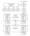
NVM Express is based on a paired Submission and Completion Queue mechanism.
- NVM Express is based on a paired Submission and Completion Queue mechanism.
- Commands are placed by host software into a Submission Queue.
- Completions are placed into the associated Completion Queue by the controller.
- Multiple Submission Queues may utilize the same Completion Queue. Submission and Completion Queues are allocated in host memory.
- An Admin Submission and associated Completion Queue exist for the purpose of controller management and control (e.g., creation and deletion of I/O Submission and Completion Queues, aborting commands, etc.) Only commands that are part of the Admin Command Set may be submitted to the Admin Submission Queue.
- An I/O Command Set is used with an I/O queue pair.
- This specification defines one I/O Command Set, named the NVM Command Set. The host selects one I/O Command Set that is used for all I/O queue pairs.
Host software creates queues, up to the maximum supported by the controller.
- Typically the number of command queues created is based on the system configuration and anticipated workload.


TBD..................


0 Comments